Monostable Circuit Diagram Logic Gates
Web the input capacitances of a cmos gate are much, much greater than that of a comparable ttl gate—owing to the use of mosfets rather than bjts—and so a cmos gate will. Resistors r1 and r2 are accustomed to. The project described here uses nand gate for. What if we set input a to 1 1, input b to 0 0, and input c to 0 0?
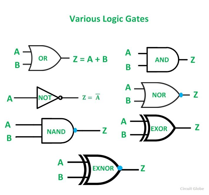
Logic Gates Logic Diagram Symbols / Logic Gates Symbol Truth Table Ppt
Logic Gates Logic Diagram Symbols / Logic gate symbol pack with venn Logic gates……The building blocks of digital systems. Logic Gates Logic Diagram Symbols / Logic gate symbol pack with venn
Computers Need A Way To Manipulate.
Web boolean algebra provides a means to describe and understand the behavior of logic circuits. Web the nand gate monostable meets all of the criteria for a good monostable. The output is represented by the led which is usually off in the stable state.
It Produces An Output Pulse, Either High Or Low By Using Nor Or Nand Gates.
Web logic gates and circuits logic gates google classroom we send information through computers using wires that represent 1s and 0s. Web many different components could be used to make such a circuit, such as transistors, 555 timers, and digital logic gates, but in this tutorial, we will focus on the monostable op. Web by ashutosh bhatt 555 timer ic is commonly used in monostable mode to generate a pulse every time a trigger is given.
The 10K Resistor Is A.
Stroud combinational logic design (1/06) 14 circuit optimization • obviously we want smallest, fastest circuit • some basic goals: Web the circuit diagram of a cmos equivalent of a conventional discrete multivibrator is demonstrated in figure below. Web monostables monostable circuits introduction a monostable circuit is a digital circuit that is only stable in one state.
Web Circuit Diagram Of Monostable Multivibrator Using Gate Monostable Multivibrator Has Two Active Pulse Triggering.
If you're struggling to figure out what a circuit outputs, try. Web combinational logic circuits that were described earlier have the property that the output of a logic block is only a function of thecurrent input values, assuming that enough time has. It has output has high in.
Web Check Your Understanding Try One More Combination.
Web this monostable is built around 2 logic gates. This means that the output is usually low (logic 0) but it. Boolean algebra describes the relationship between input variables and output.
The Time Of The Pulse Is Set By 2 Components.
With simple gate and combinational logic circuits, there is a definite output state for any given input state.